
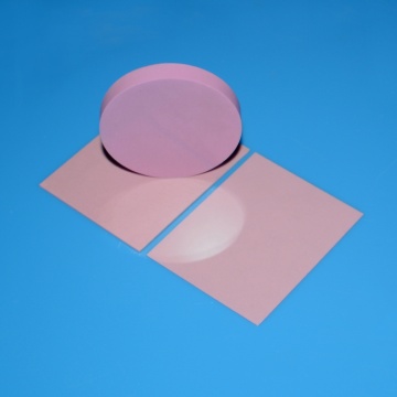
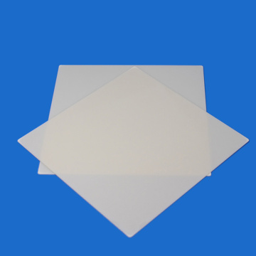
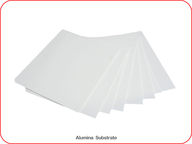
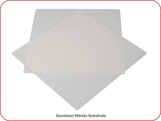
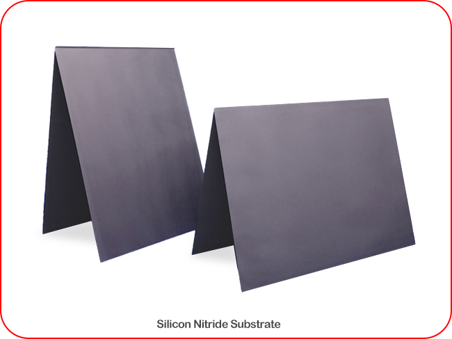
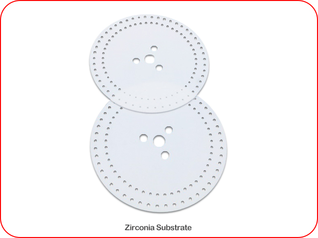
Ceramic Substrates are skinny sheets made from Advanced Ceramics. The materials used mainly include aluminum oxide (Al2O3), aluminum nitride (AlN), Silicon Nitride (Si3N4), zirconium oxide (ZrO2), and zirconium toughen alumina (ZTA).
Compared with traditional resin and metal substrates, ceramic substrates have higher electrical insulation, high thermal conductivity, mechanical strength, corrosion and erosion resistance, and unmatched high-temperature stability. The following is a comparison table of several typical material properties for reference, and you can determine which material is more suitable for your needs and applications.
| Material | Flexural strength (MPa) | Fracture toughness (MPam1/2) | Thermal expansivity (10-6/K) | Thermal conductivity (W/m.K) | Dielectric strength (KV/mm) |
| Al2O3 | ≧380 | ≧4.3 | 6.6~7.5 | ≧24 | ≧15 |
| AlN | ≧450 | ≧4.0 | 4.4~4.8 | ≧180 | ≧17 |
| Si3N4 | ≧700 | ≧6.7 | 2.7~4.0 | ≧80 | ≧20 |
| ZrO2 | ≧800 | ≧6.5 | 8.0~9.5 | ≧3 | ≧10 |
| ZTA | ≧625 | ≧5.0 | 7.0~9.0 | ≧26 | ≧25 |
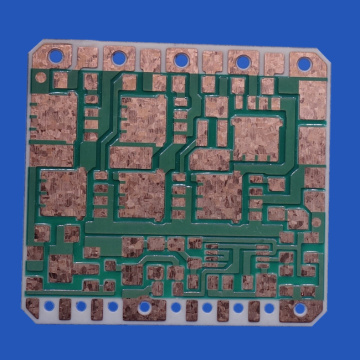
Due to the great combination of ceramic substrates' thermal, insulating, mechanical, and chemical properties has been extensively used in consumer electronics, LED substrates, automotive, telecommunications, power generation, medical, semiconductor packaging, etc.


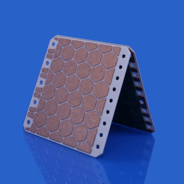


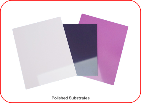
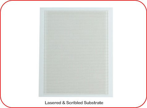
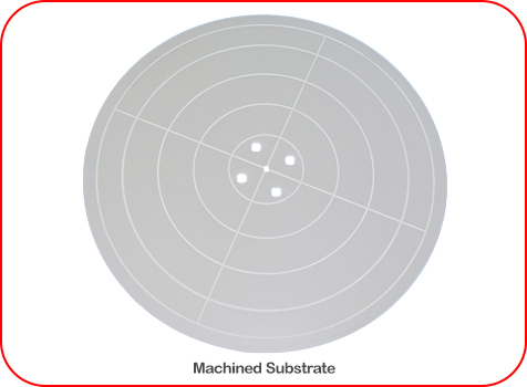
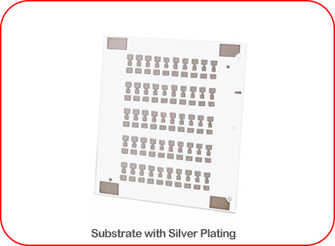
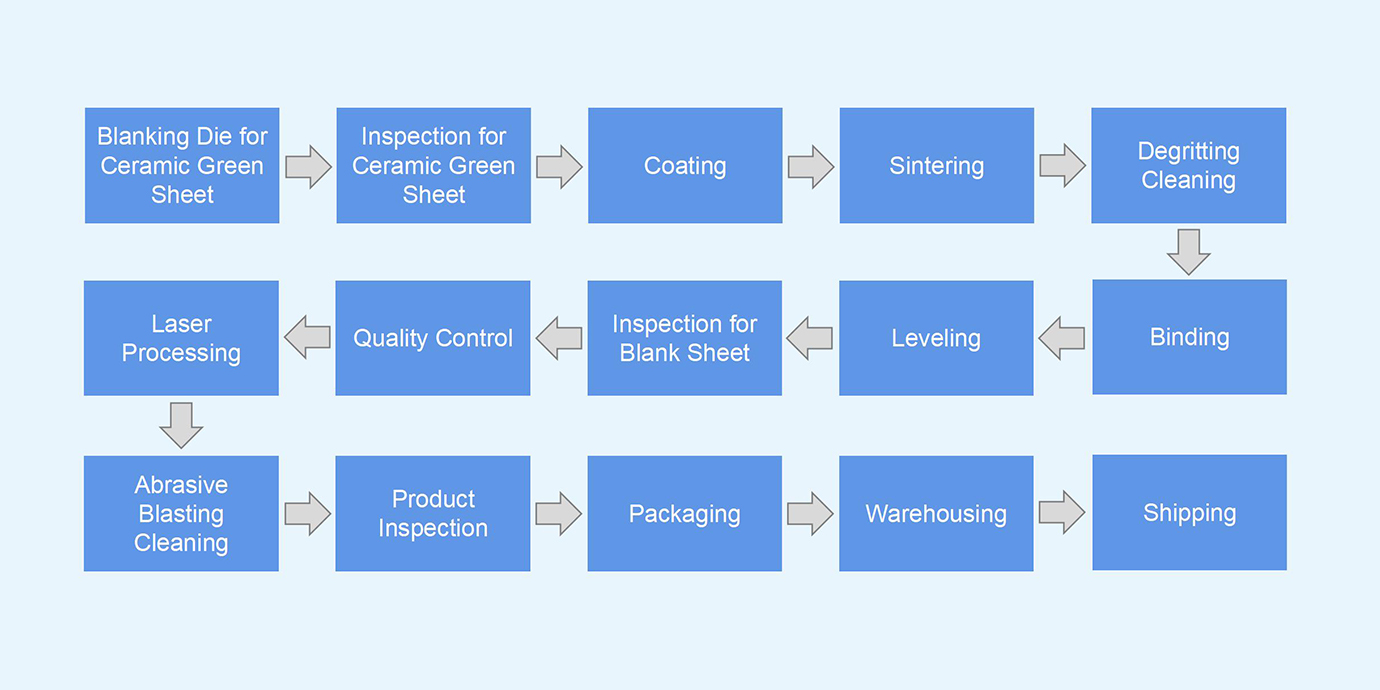


Here is our process flow.